
Developments since 2003
Process technologies — from 1 um to 0.18 um
Maximum memory capacity - 0.5-2 Mbit
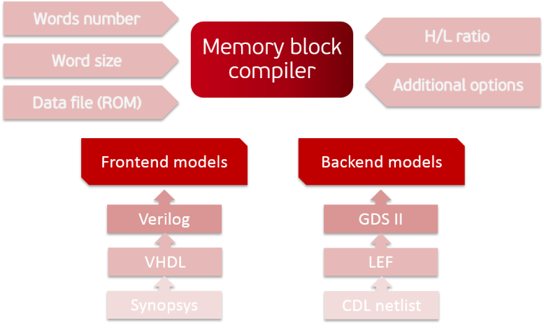
Memory block compiler is a software application used to generate a memory block for a specific technology process corresponding to the required parameters:
Memory block compilers generate memory blocks of a required shape and optimized by area for specific operating frequency and operating conditions. While generating the ROM block is programmed according to the file provided by the customer. Generated memory blocks are usually used as insertion units while microcircuits development. An option of designing a memory block as a separate microcircuit is also available.
Frontend memory compiler creates a set of memory models used while logical simulation and project synthesis (Verilog, VHDL, Synopsys). The models contain all necessary timing parameters and power consumption. At the early project’s stage a customer can choose a memory block and use the necessary Front End models.
Backend memory block compiler creates layouts of memory blocks in GDSII format and a circuit description (cdl netlist). LEF file of a developed block is included in the set of models. (LEF is a standard layout format used in place-and-route).